
1. Industry Misconception: Reflectivity Measurement Using D8-SR
Misconception
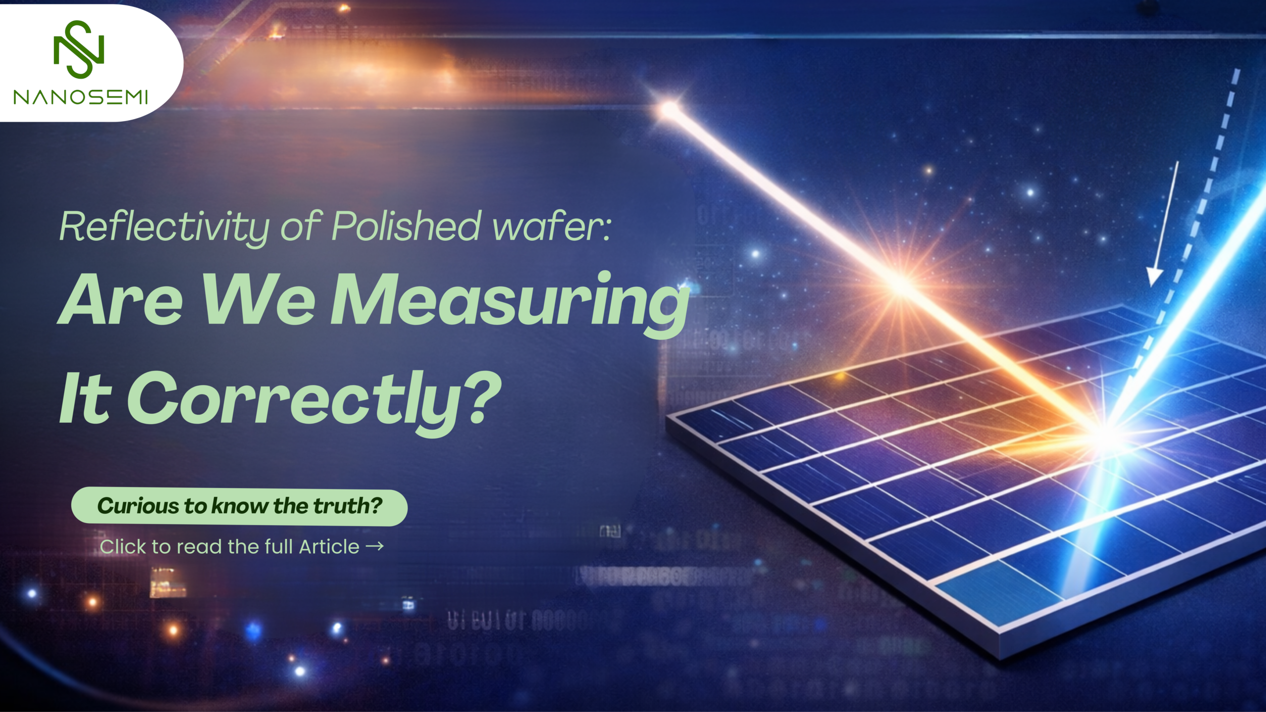
There is a common misunderstanding in the photovoltaic industry that the D8 spectroscopy reflectometer can accurately measure the reflectivity of mirror-polished silicon wafer surfaces.
Technical Reality
The D8 system is primarily designed for measuring diffuse reflectance from textured or rough surfaces, such as pyramid-textured silicon wafers commonly used in solar cell manufacturing.
The instrument typically operates using a d/8° optical geometry, which is optimized for low reflectance surfaces (generally ~10%) where light is scattered diffusely.
However, on a highly polished silicon surface, light behaves differently:
- The surface produces specular (mirror-like) reflection
- Most of the reflected light travels in a single direction
- The D8 optical system is designed to capture diffuse reflection, not pure specular reflection
As a result, measurements taken on polished surfaces using the D8 can produce unstable, inaccurate, or misleading reflectivity values.
2. D8 Technology – Working Principle
The D8 reflectometer operates using a photometric optical reflectance measurement method.
Measurement Process
- A controlled light beam is directed onto the wafer surface.
- The wafer surface reflects a portion of the incident light.
- Sensors detect the reflected light intensity.
- Reflectivity (%) is calculated based on the ratio of reflected light to incident light.
Simplified Explanation
The D8 instrument measures how much light is reflected from a solar cell surface in order to evaluate:
- Surface texturing quality
- Optical performance
- Texture uniformity across the wafer
This makes it particularly valuable for process monitoring in photovoltaic manufacturing lines.
Standard Followed
- ISO 7724/1
- DIN 5033 Teil 7
- ASTM E 1164
3. IEC Standards Related to Reflectivity Measurement
The International Electrotechnical Commission (IEC) provides guidelines for optical characterization in photovoltaic manufacturing.
IEC standards focus primarily on reflectance measurements that are relevant to device performance, including:
- Textured silicon wafers
- Anti-Reflection Coating (ARC) layers
- Finished solar cell surfaces
These measurements are important for ensuring repeatability, comparability, and production control.
However, reflectivity measurement of polished wafers is not required under IEC standards, because polished wafers are considered intermediate substrates, not the final functional surface of a solar cell.
4. Typical Applications of the D8 System
The D8 reflectometer is widely used in photovoltaic manufacturing for the following applications:
✔ Inspection of textured silicon wafers
✔ Anti-Reflection Coating (ARC) quality verification
✔ Texture uniformity monitoring
✔ Inline and offline process control
✔ Reflectance mapping across the wafer surface
Limitations
The D8 system is not suitable for measuring the reflectivity of mirror-polished silicon surfaces, due to the dominance of specular reflection.
5. Technical Capabilities of the D8 System
The D8 reflectometer provides several advantages in solar cell manufacturing environments:
- Fast, non-contact reflectance measurements
- High-throughput compatibility for production lines
- Reflectance mapping for surface uniformity
- Statistical process control (SPC) support
However, the instrument has certain limitations.
What D8 Cannot Measure
The D8 system is not capable of accurately measuring:
- Nanoscale surface roughness
- Microstructural surface features
- True specular reflectivity of polished silicon surfaces
Using the D8 for such measurements may lead to incorrect interpretations of wafer surface quality.
6. Alternative Characterization Methods for Polished Surfaces
Since the D8 reflectometer is not designed for mirror-polished surfaces, other analytical techniques should be used.
(A) Surface Roughness Analysis – SEM
Scanning Electron Microscope (SEM)
SEM provides high-resolution imaging of wafer surfaces and allows detailed analysis of surface morphology.
Capabilities include:
- Visualization of micro- and nanoscale surface structures
- Measurement of surface roughness
- Evaluation of polishing quality
✔ Highly suitable for mirror-polished wafer analysis
(B) Structural Analysis – TEM
Transmission Electron Microscope (TEM)
TEM enables analysis of ultra-fine structures and interfaces within materials.
Applications include:
- Investigation of crystal structure
- Analysis of pyramid density and interface layers
- Detailed microstructural characterization
✔ Ideal for advanced structural studies, though generally not suitable for inline production monitoring.
7. Is Reflectivity Measurement of Polished Surfaces Necessary?
Short Answer: No
Technical Reason
Polished silicon surfaces are not the functional optical surface in solar cells.
During solar cell fabrication:
- Wafers undergo surface texturing
- Texturing creates micro-pyramids that trap incoming light
- This significantly reduces reflectance and improves light absorption
Because of this, the reflectivity of a polished wafer does not directly correlate with final solar cell efficiency.
The optical performance of the final device is determined by textured surfaces and passivation layers, not the initial polished substrate.
8. Conclusion
The D8 spectroscopy reflectometer is a valuable process monitoring tool in photovoltaic manufacturing, particularly for evaluating textured and anti-reflection-coated solar cell surfaces where diffuse reflectance is relevant to device performance.
However, applying the D8 system to mirror-polished silicon surfaces results in misleading reflectivity values due to the dominance of specular reflection, which falls outside the measurement capability of the instrument’s optical geometry.
For accurate evaluation of polished wafer surfaces, direct surface characterization techniques such as SEM and TEM should be used.
From a manufacturing perspective, reflectivity measurement of polished wafers is unnecessary, since the final optical performance of solar cells depends primarily on the properties of textured, passivated, and coated surfaces rather than the intermediate polished substrate.
Jitendra Singh & Shyam Sundar Sau
Nanosemi Tech Solution Pvt. Ltd
ALSO READ : How Advanced Wafer Testing Is Powering the Next Wave of Solar Efficiency