
How India Is Building Its Semiconductor Future
A Deep Dive into India’s Semiconductor Mission and Its Path to Global Chip Manufacturing Leadership
Introduction
Semiconductors are often called the “brain” of every modern device from smartphones and laptops to cars, defence systems, and artificial intelligence hardware. For decades, India remained a peripheral player in this trillion-dollar global industry, importing nearly all its chips while exporting mostly assembled electronics. That story is changing fast.
Over the last few years, India has launched two landmark policy interventions the India Semiconductor Mission (ISM) 1.0 and its successor, Semicon 2.0 designed to transform the country from an electronics assembler into a genuine semiconductor design and manufacturing hub. This document breaks down what these two missions are, why they matter, how far India has already come, and what lies ahead.
The Backdrop: Why India Needed a Semiconductor Mission
Before ISM 1.0, India’s semiconductor-related device exports hovered at roughly $500 million per annum a tiny fraction of global trade in chips and components. Nearly all advanced semiconductors used in Indian electronics, telecom, and defence equipment were imported, exposing the country to serious supply-chain risks. The COVID-19 pandemic and the global chip shortage of 2021 made this vulnerability impossible to ignore: entire automobile and electronics production lines around the world ground to a halt for want of chips.
At the same time, India’s broader electronics manufacturing story was already gaining momentum. As the infographic below shows, India’s electronics exports grew 8-fold in a decade from ₹380 billion in 2014–15 to ₹3.3 trillion in 2024–25 thanks to programmes like Make in India and the Production Linked Incentive (PLI) scheme. Semiconductors were the natural next frontier.
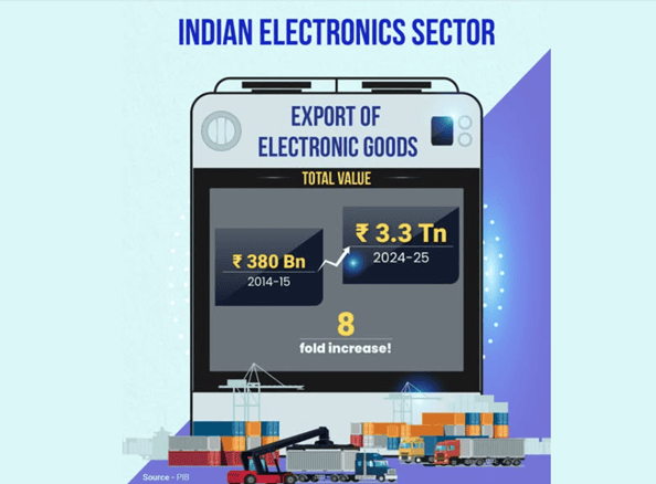
Source: PIB — India’s electronics exports have grown 8-fold, from ₹380 billion (2014–15) to ₹3.3 trillion (2024–25).
ISM 1.0: Laying the Foundation (2021 Onwards)
The India Semiconductor Mission (ISM), launched under the broader Semicon India Programme, was approved with a fiscal outlay of ₹76,000 crore. Its goal was to build an end-to-end semiconductor and display manufacturing ecosystem in the country, covering everything from chip fabrication (fabs) to design and packaging.
Key Features of ISM 1.0
- ₹64,000 crore earmarked for setting up chip fabrication (fab) units
- ₹10,000 crore allocated for semiconductor and display fab-related infrastructure and labs
- ₹1,000 crore dedicated to the Design-Linked Incentive (DLI) scheme, supporting domestic chip-design startups
- Focus on attracting global and domestic investors to set up fabs, Outsourced Semiconductor Assembly and Test (OSAT) units, and Assembly, Testing, Marking and Packaging (ATMP) facilities across states
The Results
By the time ISM 1.0 neared completion, the government had approved around 10–12 semiconductor projects, drawing a combined investment of roughly ₹1.6–1.64 lakh crore, spread across states including Gujarat, Assam, Uttar Pradesh, Punjab, Odisha, and Andhra Pradesh. A major share of this investment came from domestic conglomerate Tata Electronics and its semiconductor arm, alongside global and joint-venture partners. India also inaugurated its first Outsourced Semiconductor Assembly and Test (OSAT) facility including the CG Semi OSAT plant in Sanand, Gujarat marking the country’s entry into actual chip packaging and testing at scale.
In short, ISM 1.0 was about capacity creation: getting fabs and OSAT units off the ground, building the initial ecosystem, and proving that India could attract serious semiconductor investment.
Semicon 2.0: From Capacity to Consolidation and Depth
Building on this foundation, the Union Cabinet approved the next phase Semicon 2.0 with a much larger fiscal outlay of ₹1,27,500 crore. If ISM 1.0 was about getting the ecosystem started, Semicon 2.0 is about deepening it: moving from policy formulation and basic capacity-building toward technological depth, indigenous IP, and global supply-chain integration.
Six Strategic Pillars of Semicon 2.0
- Advanced chip manufacturing — a roadmap toward producing chips at advanced 3-nanometre and 2-nanometre technology nodes
- Full-stack Indian semiconductor IP — supporting Indian-owned intellectual property for chipsets, with companies incorporated in India retaining the IP rights
- Equipment and materials manufacturing — incentivizing domestic production of the specialty chemicals, gases, and manufacturing equipment that fabs depend on
- Design ecosystem deepening — building blocks such as compute, memory, power, networking, RF, and sensors for chip and System-on-Chip (SoC) design
- Startup and MSME support — seed/risk capital and Electronic Design Automation (EDA) tool access for smaller design players, plus deployment-linked incentives to offset the high cost of tape-outs
- Supply-chain resilience — strengthening both domestic and global semiconductor supply chains, positioning India as a dependable partner rather than just a consumer market
According to government officials, Semicon 2.0 will also give significant support to full end-to-end product development chipsets designed in India, with IP residing in India, built by India-incorporated companies extending across sectors from automotive and consumer electronics to medical devices and defence.
The Union Budget 2026–27 further reinforced this direction, with a dedicated India Semiconductor Mission 2.0 allocation of ₹1,000 crore for FY 2026–27, aimed specifically at industry-led research and training centres to build a future-ready, skilled semiconductor workforce. India is targeting the capability to design and manufacture chips for nearly 70–75% of its domestic applications by 2029, with the broader semiconductor market projected to reach $100–110 billion by 2030.
M 1.0 vs Semicon 2.0: A Quick Comparison
Graphical Snapshot: The Growth Story in Numbers
The chart below visualizes the scale of change — both in India’s electronics export performance and in the government’s rising commitment to the semiconductor mission.
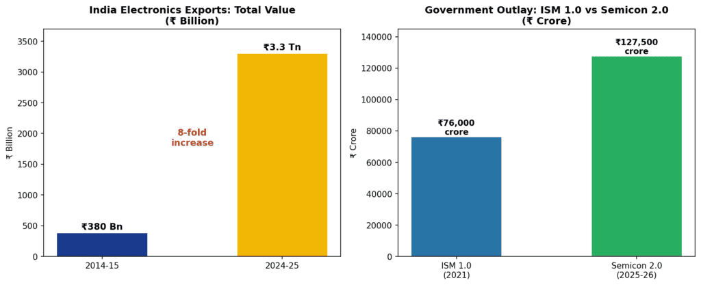
Left: Electronics exports rose 8-fold from ₹380 billion to ₹3.3 trillion. Right: Mission outlay nearly doubled from ₹76,000 crore (ISM 1.0) to ₹1,27,500 crore (Semicon 2.0).
- Left chart: India’s total electronics exports rose from ₹380 billion (2014–15) to ₹3.3 trillion (2024–25) — an 8-fold jump within a decade.
- Right chart: The government’s own semiconductor mission outlay nearly doubled from ISM 1.0’s ₹76,000 crore to Semicon 2.0’s ₹1,27,500 crore, reflecting the shift from experimentation to serious, sustained investment.
It’s also worth remembering the starting point: India’s semiconductor-related device exports were once as small as roughly $500 million a year. Multi-billion-dollar, state-backed programmes like ISM 1.0 and now Semicon 2.0 represent an attempt to change that trajectory by orders of magnitude — not just growing exports, but building the domestic manufacturing and design base that generates them.
Why This Matters: The Bigger Picture
- Strategic autonomy — Reducing reliance on imported chips protects India’s telecom, defence, and critical infrastructure from global supply shocks.
- Economic multiplier — Semiconductor manufacturing creates high-value jobs and pulls in ancillary industries: chemicals, gases, precision equipment, and specialty materials.
- Global supply chain diversification — As companies look to de-risk from concentrated manufacturing hubs, India is positioning itself as a credible alternative investment destination.
- Innovation ecosystem — Design-linked incentives and IP-focused policies aim to nurture homegrown chip-design talent and startups, not just assembly-line jobs.
- Aatmanirbhar Bharat and “Make in India — Make for the World” — Semicon 2.0 explicitly links semiconductor self-reliance to India’s broader manufacturing and export ambitions.
Challenges Ahead
Despite the ambition, several hurdles remain:
- Advanced fabrication is capital- and technology-intensive; reaching 2nm–3nm nodes requires cutting-edge equipment often controlled by a handful of global suppliers.
- Skilled workforce gaps in chip design and fabrication still need to be closed — hence the emphasis on research and training centres under ISM 2.0.
- Global competition from established hubs (Taiwan, South Korea, USA, and China) and other emerging players (Vietnam, Malaysia) means India must move quickly and consistently.
Long gestation periods — semiconductor fabs typically take years to become fully operational and profitable, requiring sustained policy commitment beyond a single budget cycle .
Conclusion
India’s semiconductor journey — from a modest $500-million-a-year exporter of chip-related devices to a country now committing over ₹2 lakh crore combined across ISM 1.0 and Semicon 2.0 — reflects a clear, deliberate strategy rather than a one-off policy announcement. ISM 1.0 proved that India could attract serious fab and packaging investment; Semicon 2.0 is now pushing the country toward advanced manufacturing, indigenous IP, and a resilient, self-sufficient supply chain.
The 8-fold rise in electronics exports over the past decade shows what sustained policy support and manufacturing investment can achieve. If Semicon 2.0 delivers on its roadmap — advanced nodes, homegrown IP, and a trained workforce — India could well transition from being an electronics assembly hub to a genuine semiconductor design and manufacturing powerhouse by the end of this decade.
Sources: Press Information Bureau (PIB), India Semiconductor Mission (ism.gov.in), Union Budget 2026–27 documents, and government statements from the Ministry of Electronics and Information Technology (MeitY).
@ Nanosemi, we provide best in class auxiliary & optical testing equipment’s with proven track record in the factory. Along with high purity speciality chemicals and gasses for semiconductor fabs. Connect us to know more.
To know more please connect here
Author: Jitendra Singh | jitendra@nanosemi.in | +91-9560 265963